A single software company can spend over 💲10 Billion/year, on data centres, but not every year is the same. When all stars align, we see bursts of new technologies reaching the market simultaneously, thus restarting the purchasing super-cycle. 2022 will be just that, so let’s jump a couple of quarters ahead and see what’s on the shopping list of your favorite hyperscaler!
Friendly warning: this article is full of technical terms and jargon, so it may be hard to read if you don’t write code or haven’t assembled computers before.
Warning #2. We are at the crossroads, where mobile/desktop and servers will have to go in different directions. So the gamers may not see most of these technologies next year.
This article was posted on HackerNews. More than once.
The original article contained around 2'700 words but was later extended at readers request to include a little more info on Intel and AMD CPUs.
What will we cover?
A lot, but not all!
First of all, this is not about emerging analogue computing technologies, quantum or optical. Those are excellent topics for research but won’t have wide adoption in the next couple of years.
Secondly, it’s not about lithography. At least not directly. We still have some headroom with the Moore’s law, so the transistors should continue shrinking. ASMLs Extreme Ultraviolet Lithography printing machines are becoming more common. TSMC was already printing at 5nm for Apple and announced 3nm coming soon. That shrinking will have a somewhat uniform effect on performance across applications, so we can save time and research something else.
Let’s focus on the devices themselves, how motherboards, RAM, SSDs, NICs, CPUs, and GPUs are constrained today and how will they evolve in the future.
Connectivity
There was a time the CPU was alone, Nowhere to go and no place to call home… SoundCloud
Connectivity is essential. All following devices are irrelevant if you can’t link them. PCI-E bus is the one responsible for that. It connects CPUs to other specialized accelerator cards, like GPUs, TPUs, IPUs. With more PCI-E lanes, you can attach more devices hence analyzing more data.
| Year | x16 Throughput | |
|---|---|---|
| Gen 1. | 2003 | 4 GB/s |
| Gen 2. | 2007 | 8 GB/s |
| Gen 3. | 2010 | 16 GB/s |
| Gen 4. | 2017 | 32 GB/s |
| Gen 5. | 2019 | 64 GB/s |
Technically, Gen 5 was introduced in 2019, but the first products started popping up in Q3 2021. Next year we expect wide adoption and a possible introduction of Gen 6 with another bitrate doubling, as always.
Assume you have a few modern GPUs like the Nvidia A100 in your system.
Each can fetch over 1 TB/s from its’s ginormous 80 GB HBM2 pack, but the CPU still easily has 20x more memory volume.
When we try to unify those pools, the non-uniformity of access latency will kill every supercomputing ambition you had as a child.
Latency aside, the 64 GB/s bandwidth in Gen 5 is still at least 16x slower, than what we would call uniform!
Compute Express Link (CXL)
This may be news to software developers, but hardware enterprises are familiar with that bottleneck and have been trying to replace or extend PCI-E for a decade now. A notable example would be the Coherent Accelerator Processor Interface (CAPI). Proposed by IBM in 2014, it was one of the first expansion buses layered on top of PCI-Express. It means the bandwidth can’t exceed the underlying protocol, only functionality, like supporting transactions between different ISA components. Intel followed up a year later with Omni-Path. Just like IBM, their effort was short-lived. Sadly, even organizing a consortium with companies like AMD, ARM, Huawei, Qualcomm and Xilinx wouldn’t guarantee the future of such proposals. The Cache Coherent Interconnect for Accelerators (CCIX) was just that…
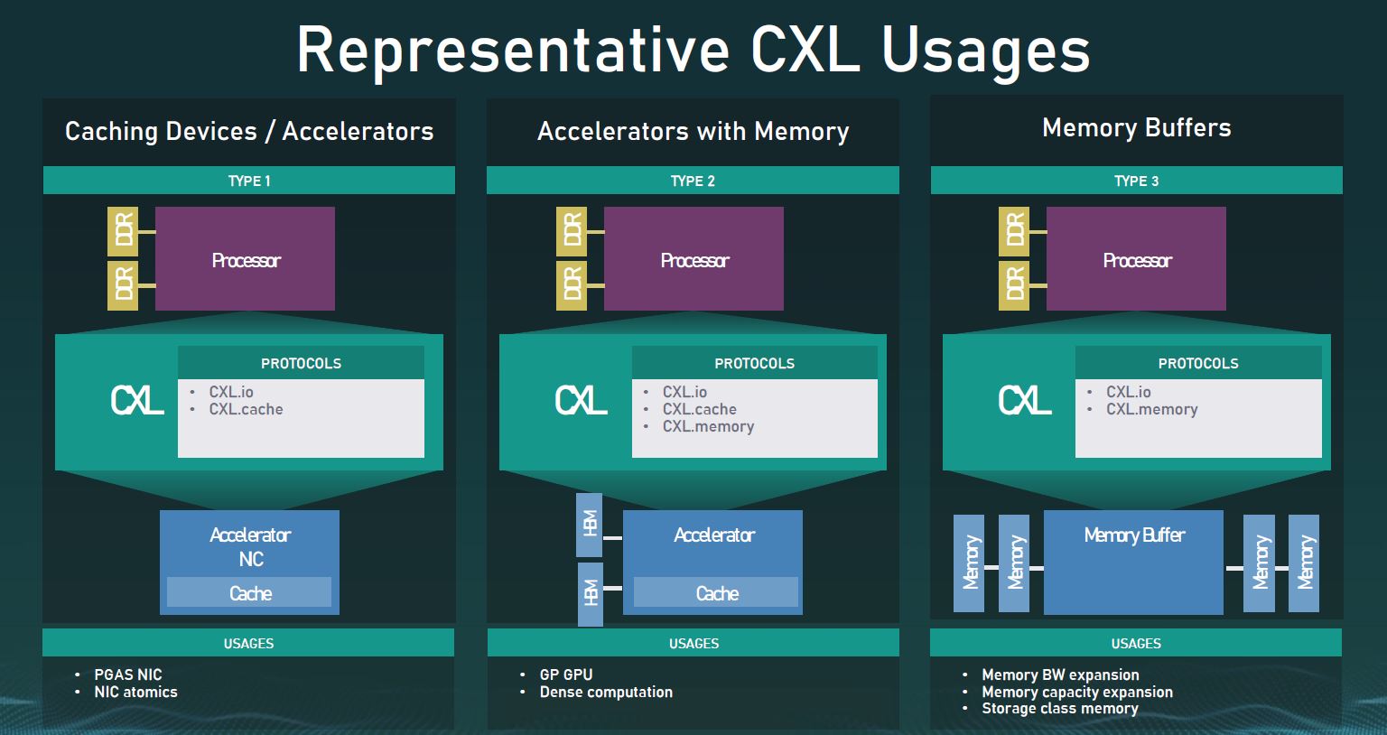
Everyone failed until someone didn’t. CXL is also extending the existing PCI-E. It already has some industry adoption. It defines three typical use cases in the 1.1 version. As we saw at the OCP Summit, tech giants are already using it for expandable memory pools. Samsungs Scalable Memory Development Kit is an excellent example of this new family of devices. It lets you attach pools of DRAM over PCI-E. Each of them becomes something like a NUMA node.
Aside from DRAM expansion and smarter NICs, CXL also hopes to revolutionize how we view and share the memory pools already installed in your chips. Today, every device has its own address space. Transparently unified addressing is extremely slow for randomized memory patterns and causes unpredictable latencies. So if your GPU has 10'000 cores and if at least 1 core in every cluster accesses remote memory, your overall speed will fall dramatically, even if 99% of cores are addressing local HBM2 buffers. Writing manual synchronization primitives has been the only solution for Unum so far, but most teams can’t bear this burden. Even the biggest game-design agencies abandoned the idea of SLI many years, because of the sheer complexity of scheduling asynchronous transfers.
Shameless plug here. We have experience with Nvidia’s CUDA queues and Cooperative Groups, OpenCL & OpenGL and Vulkan queues, and a little with SyCL. I don’t know which one is worse, but none of them is good. Vulkan is overly complex and more graphics-oriented. Everything else sucks for multi-GPU. Let us know if there is a new driver-level (not a library) async task scheduling game in town. Prefereably, a userspace framework like PMDK and SPDK. We will be happy to participate in the design!
NV-Link
We remember that CXL builds on top of PCI-E, thus inheriting parent protocols limitations. There is another game in town - NV-Link and NV-Switch by NVidia. They have 640 GB of High Bandwidth Memory spread across eight GPUs in every DGX A100 server. It must be wired together, so they have a switch inside each server!
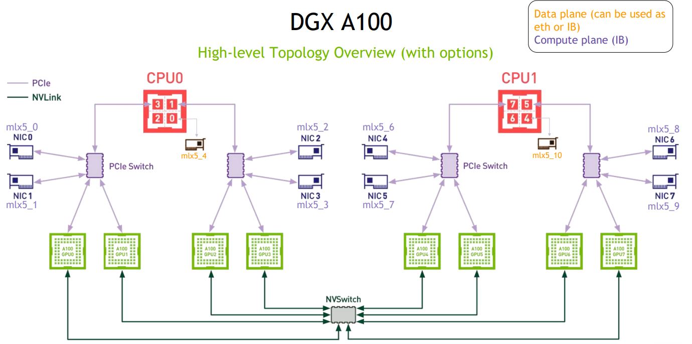
Wait, what?! A Switch. Inside of a server. 🤯🤯🤯 They have buried the consumer-level SLI and replaced it with NV-Link for pro-sumers and datacenters. That’s how you join pairs of GPUs. Each pair can then exchange 600 GB/s. A significant upgrade over PCI-E Gen 4 at the time. The NV-Switch, in turn, is used to link up to eight GPUs in most modern servers. With modern Neural Networks often exceeding 100 GB in size, you would need to slice the networks into groups of layers, store them on different GPUs, and then route signal propagation via NCCL. NV-Switch will handle it at an aggregate throughput of 9.6 TB/s.
There is something else luring far-far ahead. Photonics! One day we will write about it! Subscribe until then!
Volatile Memory: DDR5
With 1 TB RAM per AMD Epyc CPU, it would take over 5 seconds just to memset the whole memory at peak 200 GB/s speed.
Too slow, so DDR5 comes to the rescue.
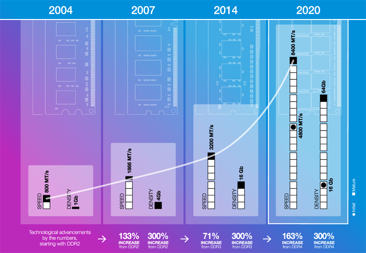
PCI-E slots are both forward and backward compatible. You can put a new GPU into an old slot and vice versa. The same doesn’t hold for RAM though. New generation - new motherboards. New motherboards - new CPUs. So it’s less surprising that DDR4 was with us from 2014 until now, 2021.
A big datacenter hosts about 200'000 CPUs. At 💲5'000 per CPU — vendors can’t afford fashion for the sake of fashion. A replacement of CPUs alone would cost 💲1 Billion, so it must be justified. So how much better DDR5 is:
- Clock rate: from 1.6 GHz up to 4.8 GHz.
- DIMM size: from 64 GB to 256 GB.
I would expect double the speed, quadrupled volume, and better power efficiency. We can already taste such rates in the new MacBook Pro 2021. This 💲2'000 marvelous piece of engineering packages DDR5 with 400 GB/s bandwidth, double what you get in a 💲200'000 state-of-the-art server.
Persistent Storage
First of all, isn’t it weird that we still sell NVME SSDs in the M.2 form-factor? They are tiny and make sense for laptops, but why put the same in the server?
If you thing it’s odd, the U.2 is batshit crazy.
It’s designed to fit into the 2.5" caddies of most servers, which are inherited from the old HDD days.
We had Large-Form-Factor 3.5" HDDs from 1983 and the newer Small-Form-Factor 2.5" HDDs since 1988.
That technology used magnetic spinning disks and was capped at 20 MB capacity.
Our current U.2 Samsung M393AAG40M32-CAE SSDs each have 8 TB (300'000x more) in the same form factor without any spinning disks involved.
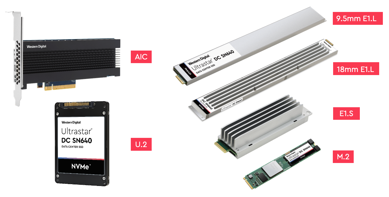
In 2022 we will finally start fixing that historical joke. The replacement isn’t without quirks - too many sizes, but I appreciate the change. Here we see two significant trends:
- removal of caddies — one less part to buy from vendors,
- hot-pluggable PCI-E devices — so it’s easier to replace and service,
- longer and slimmer body, to make more capacity serviceable from the server front,
- taller heatsinks for next-generation controllers with up to 40W expected power consumption.
New SSDs will sit on the PCI-E bus, so the controllers should become faster. Today’s record is about 7 GB/s and can’t be above 8 GB/s. In the next-gen, the cap will be 16 GB/s.
Furthermore, did you know modern SSDs also house logic and volatile memory on board? The cheap ones cut the costs and may have no DRAM aboard. Write performance then becomes inconsistent but may stay unnoticeable for some users. With higher connectivity, this bottleneck may be gone. SSDs can lose logic and RAM and solely provide block-addressable NAND flash arrays. All the magic can then move to userspace software, potentially eradicating the filesystem concept — worth exploring.
Persistent… Memory?
There is more. Volatile and persistent memory have radically different bandwidths and volumes. The first is small and fast, and the second is big and slow. The gap is enormous, with about 10'000x speed difference in randomized mixed read+write operations. Software vendors are trying to reduce this gap, but the hardware is also evolving.
Meet “Persistent Memory” — the foster child of Intel and Micron. Though promising, the unit went through multiple reorganizations in the last few years and only gained traction now.
The main promises PMem brings, are:
- Zero boot time. Your RAM essentially becomes persistent. Once the computer is turned on - you don’t need to boot. All the applications continue from the same place.
- Larger memory pools. The common upper bound for RAM is about 2 TB/socket today. With PMem it can be 12 TB.
Why isn’t everyone using it then?
- It’s very pricey.
- Software adjustments are needed to use it properly.
Plus, I don’t know if it works with AMD CPUs. Adoption-wise, TensorFlow has 160K stars on GitHub, but still has no proper support for AMD GPUs. PMDK has only 1K stars, so it still has much adoption to gain. Most of our servers have AMD Zen2 CPUs at Unum, and we have no PMem to experiment. Maybe next year!
Smart NICs and DPUs
SmartNICs are weird and very hard for me to grasp. As clouds grow and software-defined networking becomes a thing - companies like Amazon start cramming more stuff into networking cards. We know little about such a scale and the use case.
Down here on Earth, we love training big Deep Learning models. After showing a randomly sampled batch of data to a neural network on one server, you use gradients to guide the change of weights towards finding the minimum of the loss (error) function. Like most classical distributed computing, you split your machines into “masters” and “slaves”. The “managers” and number-crunchers, but suddenly “managers” end up doing just as much arithmetics - averaging the state across the cluster after every batch and broadcasting it back.
With 200 Gbit fibres today and 400 Gbit fibres tomorrow, sending the data to neighboring machines becomes cheaper, while averaging becomes more noticeable. So the industry answer is to put more RAM, CPU cores and GPUs into the NIC, making it a server by itself.
- DPU will run a separate instance of Linux.
- DPU will have it’s own processes and address space.
- DPU will even have a separate management LAN.
Genuinely, the overall concept doesn’t make sense to me. It may do the job in some cases, but I would hardly call it future-proof or elegant. The time will tell!
CPUs & GPUs
Finally, we reach the coolest part of the review - CPUs & GPUs. Those two generally work in tandem and are the pillars of modern High-Performance Computing. We have seen Systems-On-a-Chip (SoC) that pack both on a single die, but that’s mostly for laptops and entry-level gaming.
AMD
The CPU is flat. At least that’s how “they” want us to think. 😁 It wasn’t flat before, and it’s most definitely not now. AMD already has a colossal socket, so when they tried to grow memory, they decided to stack it on top - vertically. Hence the name. V-Cache was recently announced for desktop Ryzen CPUs, tripling the L3 cache size of the fastest desktop CPU. Our top-of-the-line Epyc and Threadripper Pro CPUs have 256 MB of L3 cache. It’s enough, in theory, to fit the Linux kernel without even using the RAM! Next year it will likely be ≥ 768 MB! The bandwidth of L3 will grow, but the latency may increase a little.
AMD has some of the epic CPU series names on the server market. We have seen Naples (Zen 1), Rome (Zen 2), Milan (Zen 3), following are Genoa and Bergamo on Zen 4. Experienced travelers may have noticed the pattern. Every year we were traveled across Italy, further and further North. Until Genoa, which is a whopping 1° south of Milan! Customers must be furious with this atrocity, so Genoa brings massive upgrades to compensate for the disappointing name. 😁 All in a gigantic new SP5 LGA 6096 Socket.
| Milan | Genoa | Bergamo | |
|---|---|---|---|
| Cores | 64 | 96 | 128 |
| TDP | 280 W | 320 W | 320 W |
| Cache | 256 MB | 804 MB | 804 MB |
| RAM Channels | 8 | 12 | 12 |
| PCIe | 128x Gen4 | 128x Gen5 | 128x Gen5 |
| Lithography | 7nm TSMC | 5nm TSMC | 5nm TSMC |
| Availability | 2021 | 2022 | 2023 |
All of this is just a guess, of course. We can further speculate that new CPUs may support up to 12 TB of DDR5 RAM per socket. We also expect all cores to support SMT2, just like Milan and Milan-X.
The most significant core-count changes are happening in the GPU market, still.
With the grand unveiling of their MI200 GPU series, they took the lead in FP64 high-precision workloads.
Irrelevant for Machine Learning, it still underpins ballistics and some scientific computations.
Anyways, congratulations on delivering the first MCM design in GPU history!
Intel
Enthusiasts may have noticed that CPUs these days have almost as many cores as GPUs Execution Units. Their Floating Point Units are getting beefier, and the power consumption in both cases may soon surpass 500W. Looks like convergence.
So Intel thought, why not pack HBM into the product similar to how GPUs are sold? That’s precisely what’s announced for 2022 Intel Sapphire Rapids chips. It’s not clear if the system sees it as a RAM NUMA or an L4 cache, but I am eager to see!
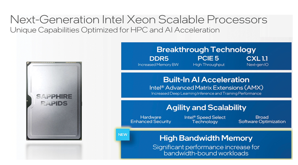
Innovations also include the expected switch to DDR5, PCIe Gen5 (with support of CXL) and a new UPI link.
Less conspicuous yet predictable arrive the AMX SIMD instructions.
Those manipulate 64 byte registers, just like AVX-512, but focus only on matrix multiplications.
If Nvidia Tensor Cores already support TF32, FP64, FP16 and many other numeric types, Intel only focuses on AI inference for now - INT8 and BF16.
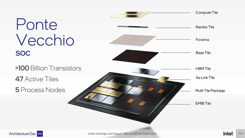
Just like AMD, Intel isn’t done with GPUs. Ponte Vecchio, their new massive GPU, is also expected in 2022. The stakes are so high that they are going for the TSMC 5N lithography instead of their own fabs. We haven’t seen discrete GPUs from Intel in years, but somehow, on the software side, they are better prepared for heterogeneous computing. They have joined the SyCL consortium, extended their compiler toolchain, but I have to state that they are still behind Nvidia from the software perspective.
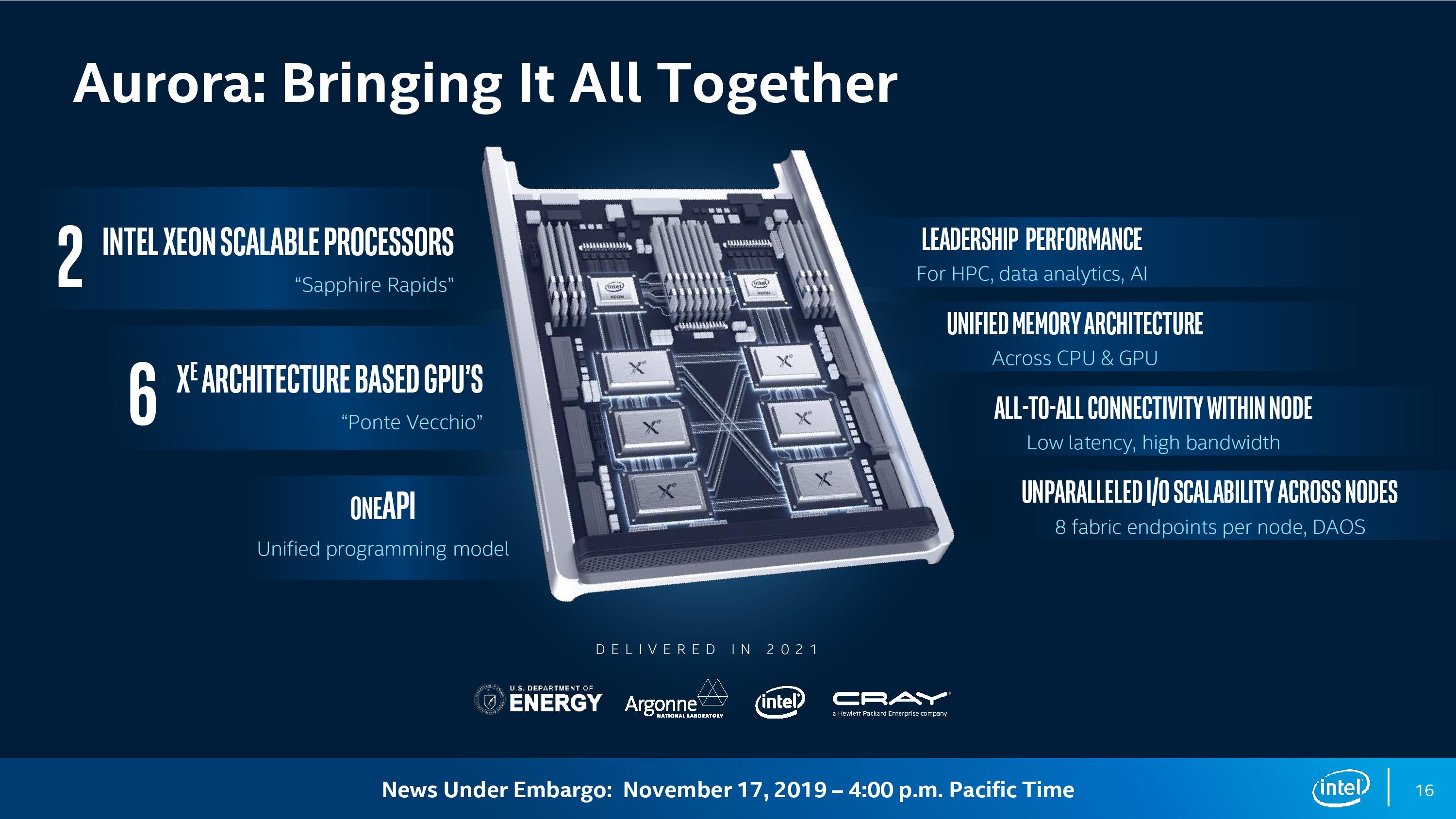
With all this preparation, it’s only natural that they unroll their all-Intel servers to compete with Nvidia DGX A100.
ARM & Nvidia
I expect broader adoption of ARM v9 ISA and availability of SVE2 SIMD extensions. The first of its kind, with runtime-defined register size. Your software will have the same binary for all hardware versions with SIMD registers ranging from 128 to 2048 bits. Todays Ampere Altra Max CPUs feature 128 cores. A single 2048-bit register would fit 128 half-precision floats. With reduced control-flow granularity and huge vectorized registers this already reminds me GPUs.
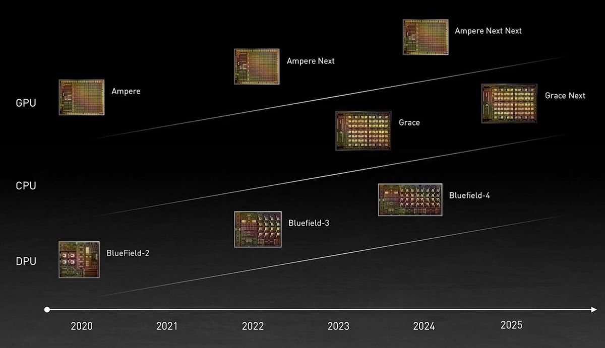
If this wasn’t enough, Nvidia is buying ARM. Everyone has known it for over a year now. Some parties protest against this deal, but they unitedly can still bring something unique to the market next year regardless of the merger. I am talking, of course, about the ARMv9 + NV-Link integration. At their last GTC conference, they talked about our favorite memory bottlenecks and how they will solve them with “Grace”! 😂
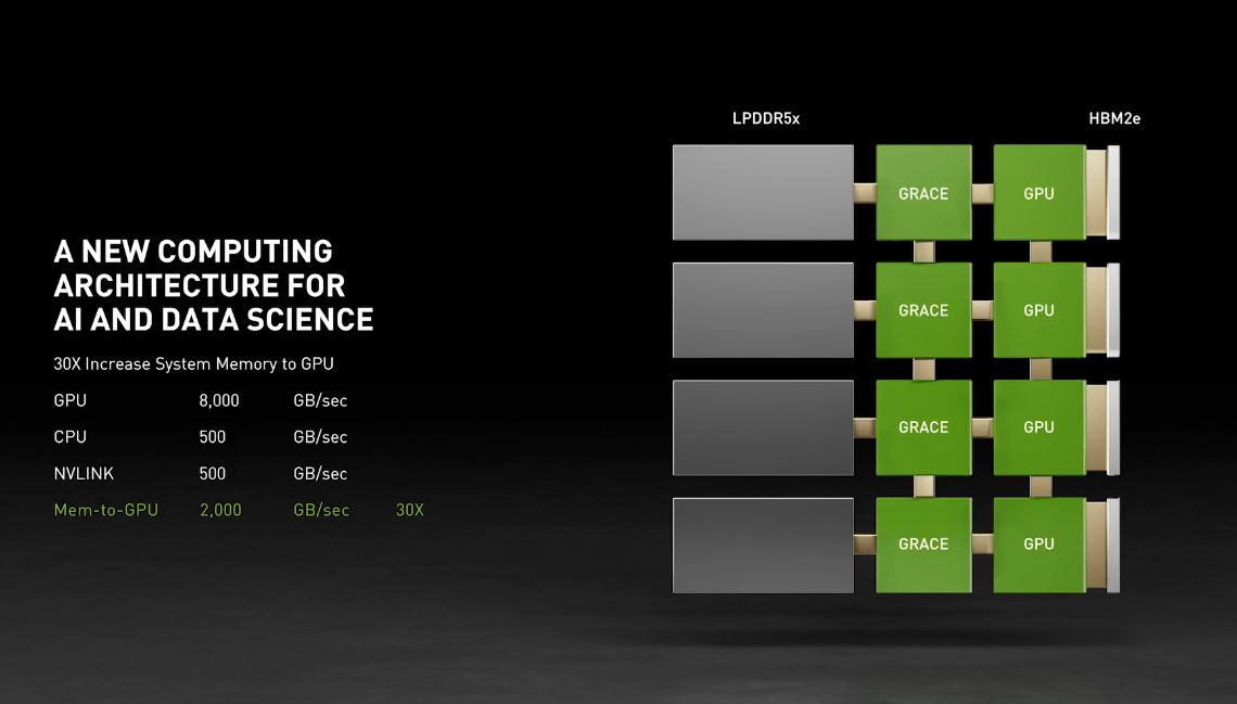
Grace is their upcoming ARM CPU paving the road for many advanced next-gen technologies. Today, the most common solution for server design for a dense environment implies two x86 sockets in 2U. Dual AMD Epyc gives you not 256 PCI-E lanes (128 x 2), but 160, as 96 would be used for inter-processor communication. 160 is enough for 8x GPUs and 8x SSDs simultaneously, but this hides the question of affinity. It’s tough to localize and reserve RAM buffers on the CPU side for a specific GPU. Aside from higher bandwidth Nvidia’s Grace concept may provide a simpler programming model. A one-to-one ratio between CPUs and GPUs looks closer to a four-node server than a single node with 4x CPUs and GPUs.
The overall landscape seems extremely promising! We haven’t seen this much variety in the hardware space since the early days of computing. This article could be much longer and detailed. Cerebras, GraphCore, SambaNova all presented exciting chips recently, and we will do our best to port our software to as many HPC platforms as possible!